AOI
AOI
AOI has functions such as component detection, PCB board detection, and welding component detection.
The general program used by the AOI inspection system for component inspection is to automatically count the printed circuit boards of installed components and start the inspection; Check the lead side of the printed circuit board to ensure that the lead ends are aligned and bent correctly; Check for missing, incorrect, or damaged parts, check the type, direction, and position of the installed IC and discrete components, and check the printing quality of the markings on the IC components.
If AOI detects defective components, the system will send a signal to the operator or trigger a processing program, which can automatically remove the defective parts. The system analyzes defects, provides the type and frequency of defects to the host, and makes necessary adjustments to the manufacturing process.
The efficiency and reliability of AOI detection depend on the integrity of the software used.
Automatic X-ray inspection utilizes the differences in different substances in X-ray absorption to inspect the parts and defects by checking 1%-2%. Mainly used to inspect defects such as extremely fine spacing, extremely high density circuit boards, bridges, missing parts, and poor alignment during the assembly process. It can also use its tomography technology to detect internal defects in IC chips. This is the only way to detect the quality of the ball grid array and solder ball welding.
Key Factors in PCBA Processing
There are several key factors that need to be noted during the PCBA processing:
1. Equipment accuracy: High precision SMT and welding equipment are the foundation for ensuring product quality. PCBA-TECH adopts advanced equipment to ensure the accuracy and stability of every step.
2. Raw material quality: High quality circuit boards and electronic components are a prerequisite for manufacturing high-performance products. PCBA-TECH strictly screens suppliers to ensure the high quality of raw materials.
3. Process control: A sound process and quality control system are key to ensuring product consistency and reliability.
PCBA-TECH has rich experience and professional knowledge, able to accurately control every process step.
Function Test
In order to verify the pcba quality,function test is necessary.
You can provide firmware, software,programming and testing procedure to us,we have computer for testing and help you make the test fixture or tool.
FCT for PCBA
FCT(Functional Circuit Test) requires IC programming, simulation testing of the entire PCBA board’s functionality, identification of hardware and software issues, and provision of necessary SMT production fixtures and testing jigs.
PCB Assembly
PCB Assembly Flow
1. Circuit board preparation: Firstly, it is necessary to prepare the circuit board, clean and dry it to ensure that the surface of the circuit board is clean and flat.
2. Solder paste printing: Use a solder paste printing machine to evenly print a thin layer of solder paste on the PCB, providing welding points for subsequent SMT patches. The uniformity and accuracy of solder paste directly affect the quality of subsequent patches.
3. Component mounting: Use an SMT mounting machine to mount electronic components to the designated location on the circuit board. This step requires high-precision equipment and skilled operators to ensure accurate installation of components.
4. Welding: By using welding equipment to weld components, the connection between the components and the circuit board is achieved. The choice of welding process will affect the quality and performance of the product. Bitelli Electronics adopts a high standard welding process to ensure the reliability of the product.
5. Testing and quality inspection: After welding is completed, the product is tested and inspected. Including electrical performance testing, appearance quality testing, etc., to ensure that the product meets design requirements.
6. Cleaning and drying: Clean and dry the PCBA board to remove impurities and moisture from the surface, and prepare for subsequent processes.
7. Finished product inspection and packaging: Finally, the finished product is inspected, qualified products are selected for packaging, and then delivered to the customer.
Components
When we get your BOM, we will check their Description and Manufacturer Part Number, if only have description,we will quote them by it and note the part number to you in our Open BOM,so it is better for us to use your part number to quote them directly.
Notes: Substitute without part number is ok,we will check the description firstly.
Coating PCB
The coating is a specially formulated material used to protect circuit boards and related equipment from environmental erosion. It has good resistance to high and low temperatures; After curing, it forms a transparent protective film that can protect the circuit from damage in situations such as chemical substances, vibration, moisture, salt mist, humidity, and high temperatures. So what are the coating processes? Let’s take a brief look below:
1、 Brush coating – widely used and can produce excellent coating effects on smooth surfaces.
2、 Automatic dip coating – dip coating ensures complete film coverage and does not cause material waste due to excessive spraying.
3、 Selective coating – Accurate coating without wasting materials, suitable for large-scale film covering, but with high requirements for coating equipment. More suitable for large-scale lamination. Using a prepared XY table can reduce masking. When painting PCB, there are many connectors that do not require painting. If the adhesive tape is too slow to apply and there is too much residual adhesive when tearing, consider making a combination cover according to the shape, size, and position of the connector, and positioning it with installation holes. Cover areas that do not require painting.
4、 Spraying – the use of spray can type products can be easily applied to maintenance and small-scale production. The spray gun is suitable for large-scale production, but these two spraying methods have high requirements for the accuracy of operation, and may produce shadows (where the lower part of the components is not covered with the coating).
The above is the coating process for PCB, hoping to be helpful to you.
AOI for PCBA
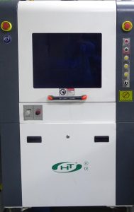
AOI is a type of testing equipment, also known as AOI optical automatic testing equipment, which has become an important testing tool and process quality control tool for ensuring product quality in the electronic manufacturing industry.
The working principle of AOI detection equipment is that during the automatic detection process, the AOI detection equipment machine automatically scans the PCBA product through a high-definition CCD camera, collects images, compares the test points with qualified parameters in the database, and after image processing, checks the solder joint defects on the target PCBA, and displays or automatically marks the defects.